India has taken a major step forward in semiconductor innovation with the launch of its first-ever 3nm chip design centers. Moreover, this initiative will strengthen India’s position in the global semiconductor industry.
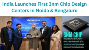
The centers were inaugurated by Union Minister Ashwini Vaishnaw and established by Renesas Electronics India. This initiative marks a significant milestone in India’s journey toward technological self-reliance and innovation in the semiconductor ecosystem.
The launch of these centers will help India compete with leading semiconductor nations and encourage research, innovation, and collaboration between industry and academia.
What is 3nm Chip Design Technology ?
3nm chip technology represents one of the most advanced semiconductor manufacturing processes currently available in the world. The term “3nm” refers to the size of the transistor structures used inside the chip, which are extremely tiny and allow billions of transistors to be packed into a single processor.
Compared to older technologies such as 5nm and 7nm chips, 3nm chips offer several important advantages:
-
Higher performance for computing and processing tasks
-
Lower energy consumption, making devices more power-efficient
-
Improved processing speed for advanced applications
-
Better performance for AI and high-performance computing
This level of innovation is critical for powering next-generation technologies such as artificial intelligence, data centers, smartphones, and advanced computing systems.
Global Recognition of India’s Semiconductor Capabilities:-
- India’s growing semiconductor capabilities are receiving recognition across global technology platforms. International companies and investors are increasingly looking at India as a promising destination for semiconductor design and development.
- Global forums such as the World Economic Forum have highlighted India’s potential in the semiconductor sector. India’s large pool of engineering talent and strong IT ecosystem make it an attractive hub for global chip design companies.
- The launch of 3nm chip design centers further strengthens this global confidence and demonstrates India’s ability to contribute to the future of semiconductor innovation.
Contribution to the Atmanirbhar Bharat Vision :-
The establishment of these advanced chip design centers also supports India’s broader vision of technological self-reliance.
Under the government’s Atmanirbhar Bharat initiative, several programs have been launched to promote domestic semiconductor development, manufacturing, and design capabilities.
By strengthening local chip design infrastructure, India aims to reduce dependence on imported semiconductor technology and build a strong domestic ecosystem.
These initiatives are expected to:
-
Promote research and development in semiconductor technology
-
Encourage startups and innovation in chip design
-
Create new employment opportunities in the technology sector
-
Strengthen India’s global technology leadership
Role of Renesas Electronics in India’s Semiconductor Growth
Renesas Electronics is one of the leading semiconductor companies globally and plays a key role in embedded semiconductor solutions.
The company sees India as a strategic market and is expanding its semiconductor design and development capabilities in the country. Through its initiatives, Renesas is supporting engineering talent, academic institutions, and startups involved in semiconductor research.
Renesas is also collaborating with universities and technical institutes to promote innovation and skill development in chip design and embedded systems.
Support Through the Chips to Startup Programme
One of the important initiatives supporting semiconductor innovation in India is the Chips to Startup (C2S) Programme.
This program focuses on providing students, startups, and researchers with access to advanced chip design tools and learning resources. By encouraging practical learning and real-world semiconductor design experience, the initiative aims to prepare a skilled workforce for the semiconductor industry.
Additionally, the Design Linked Incentive (DLI) Scheme supports semiconductor design companies and startups with financial incentives and infrastructure support.
These programs are helping India develop a strong semiconductor design ecosystem and attract global investment in the sector.
Government Initiatives Driving Semiconductor Development
The Government of India has launched several initiatives to support the growth of the semiconductor industry under the India Semiconductor Mission.
Through this mission, the government is working to build a complete semiconductor ecosystem that includes chip design, manufacturing, research, and skill development.
Key initiatives include:
-
Providing Electronic Design Automation (EDA) tools to over 270 academic institutions
-
Encouraging collaboration between universities and semiconductor companies
-
Supporting research and development in advanced chip design technologies
-
Distributing hands-on semiconductor learning kits to engineering students
These efforts aim to make India a major player in the global semiconductor value chain.
Future of Semiconductor Innovation in India
With the launch of the first 3nm chip design centers in Noida and Bengaluru, India has taken an important step toward becoming a global semiconductor innovation hub.
The country’s strong engineering talent, growing startup ecosystem, and supportive government policies are creating a favorable environment for semiconductor research and development.
Strategic partnerships with international companies and nations, including Japan, will further accelerate India’s semiconductor growth and technological leadership.
As the demand for advanced computing, artificial intelligence, and smart devices continues to grow, India’s semiconductor ecosystem is expected to play a crucial role in shaping the future of global technology.

